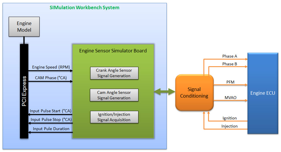
Concurrent's programmable FPGA PCIe card features a powerful field-programmable gate array with 362K or 504K logic elements that supports both digital and analog I/O. The card can control up to 96 digital I/O signals along with 16 analog inputs and 16 analog outputs. The programmable FPGA card features isolated I/O power, high-speed digital isolators and multi-board synchronization.
The FPGA Engine Sensor Simulator is an FPGA-based car engine sensor simulator card by Concurrent. This PCIe card provides functionalities such as:
The 8-channel LVDT/RVDT Simulation card is a customized version of Concurrent’s programmable FPGA card designed especially for HIL testing. Features and specifications:
|
| Firmware Selection
Set firmware for this instance of the board.
- Physical Board Instance:
Select the physical board that this panel instance will use.
The Concurrent FPGA boards have multiple functionalities,multi-function
I/O or FPGA engine sensor simulation with different firmware flavors etc., determined by the firmware
installed on the board. The same low level Linux driver is
used by all the functionality. A system can have different types of
boards installed so in this case it is necessary to tell the driver
which physical instance of the board to use for the specific SimWB
panel. The instances of the boards known to the driver can be listed
by using the Scan System utility below. This will return the Card Number of the FPGA boards and
this Card No should be mapped to the Physical Board Instance.
- System Info
Scan the system to get information of all the Concurrent 9290 cards available on the system and return
only the 9290 engine simulator card. The card number returned by the scan should be set as the Physical
Board Instance number.
- Firmware Selection and Summary
Select the right firmware file for the firmware flavor available on the FPGA board. For example if the System Info
return the FwFlv and the FwVer then select the FwFlv_FwMajorVersion_X configuration file. The Firmware configuration
file is valid for all major versions of the Firmware Flavor. Selecting the Firmware Configuration file will enable
and disable different options in the FPGA Configuration GUI. Select the Firmware Configuration file before you
start the I/O mapping. Changing the Firmware Configuration file may result in the I/O mappings being lost.
|
 |
|
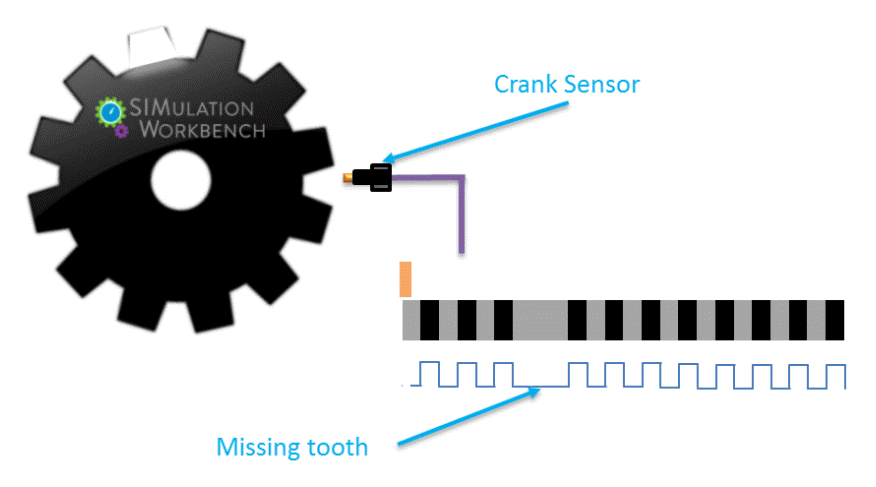
| Crank Configuration
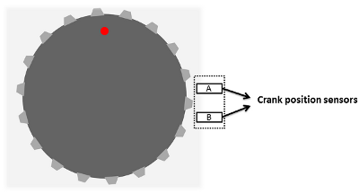
The crank position sensor configuration is assumed to be as follows:
- Num Crank Teeth: Number of crank teeth, specified as an integer in the [4 60] range.
Tip: Use the  and and  buttons to customize the crank tooth transition table. However, note that using these buttons results in values of the Num Crank Teeth and Default Tooth Size fields being inapplicable. buttons to customize the crank tooth transition table. However, note that using these buttons results in values of the Num Crank Teeth and Default Tooth Size fields being inapplicable.
You can also specify custom values for each tooth transition by double-clicking the table entry and entering the desired value. Press enter.
- Default Tooth Size: Angular width of each tooth, specified in the (0,360/num_crank_teeth)° range.
- Crank Offset: Crank initial position, specified in degrees (°).
- Crank Rotation: Crank rotation angle, specified as 360° or 720°.
- Polarity: Output crank PhaseA and PhaseB signals as Active High or Active Low.
- Note: Right-click on the table will invoke the menu to set the starting point of the tooth profile.
|
 |
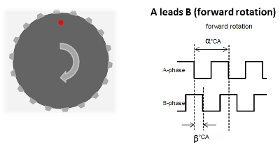
Reverse Rotation Setup
- Output on Pin0: Select Phase A or PFM to output on Pin DIO_0.
- Phase A/B
- Phase B Offset (°CA):Phase B sensor offset. Set this to half of the tooth width.
A phase offset is required to output PFM and MVAO waveforms.
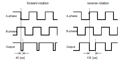
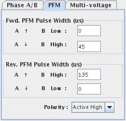
- PFM (Programmable Frequency Modulation)
Output a pulse with different width (us) for forward and reverse rotation.
- Polarity: Output PFM signal as Active High or Active Low.
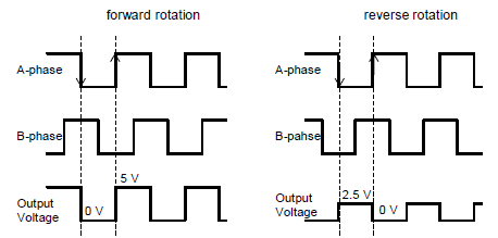
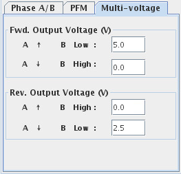
- Multi-voltage (Multi-voltage analog output). *Optional depending on firmware.
Output an analog voltage on ALG_OUT0 with different voltage levels for forward and reverse rotation.
|
|
|
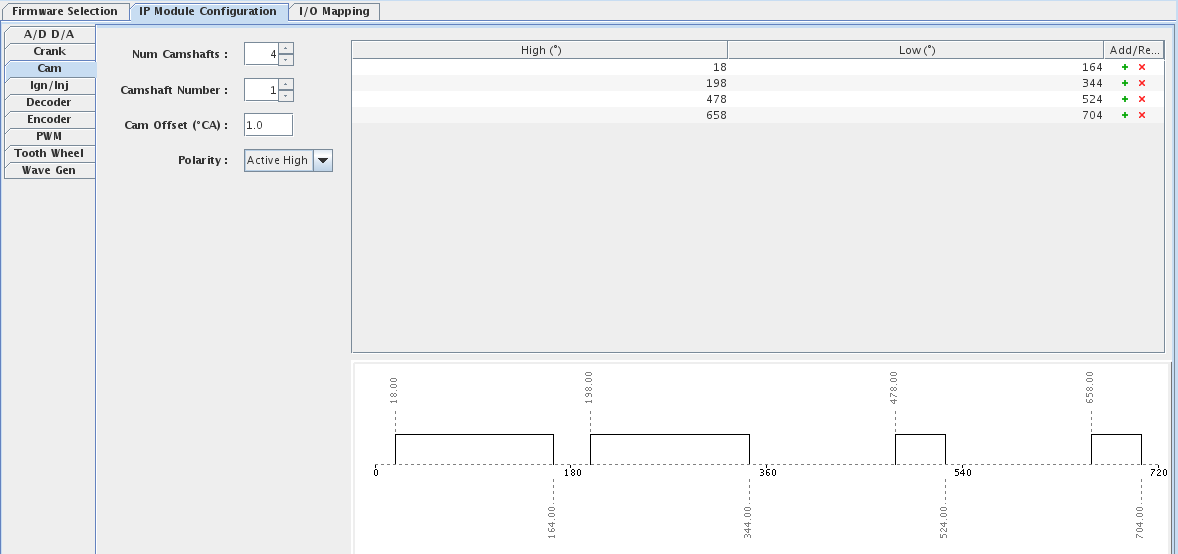
Cam Configuration:
- Num Camshafts: Number of camshafts, specified as an integer in the [1 4] range.
- Camshaft Number: Apply configuration to the selected Camshaft.
- Cam Offset: Camshaft initial position, specified in degrees (°).
- Polarity:Output Camshaft signals as Active High or Active Low.
Tip: Use the and buttons to customize the cam tooth transition table.
You can also specify custom values for each tooth transition by double-clicking the table entry and entering the desired value. Press enter.
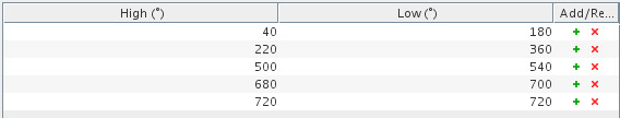
The values of High and Low °CA need to be in ascending order.
|
 |
|
|
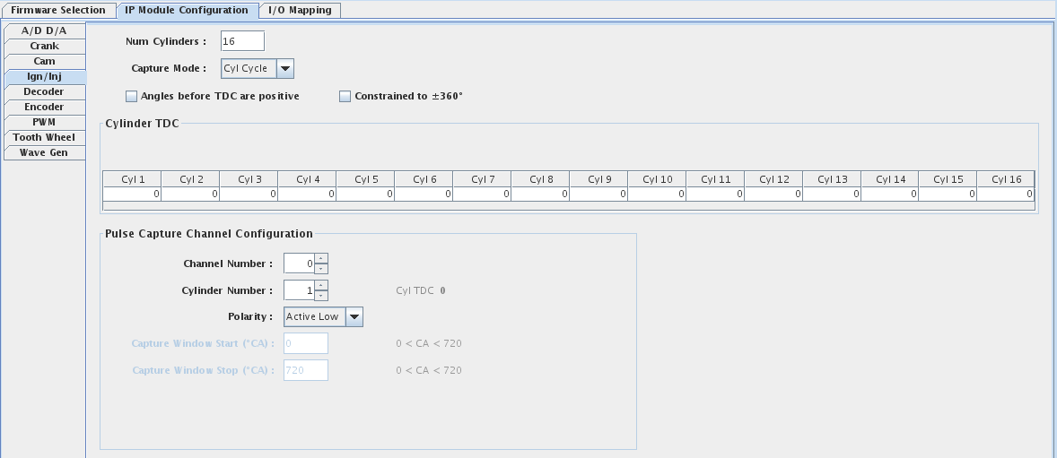
| Ign/Inj Configuration:
All channels can be used for ignition or injection pulse capture. The information captured for each channel is relative
to the TDC of the cylinder for which the channel is configured. A minimum of 8 pulse capture channels are required of
capturing the ignition and injection pulses of a 4 cylinder engine.
- Num Cylinders: Number of cylinders with a maximum of 16 cylinders.
- Cylinder TDC: Cylinder TDC for each cylinder. The Injection and Ignition input captured pulse information is offset by the specified TDC.
- Angles before TDC are positive: By default the angles before TDC are offset with TDC and negative. Selecting this options
will make angles before TDC to be positive and angles after TDC will be negative.
- Channel Number: Select a Ign/Inj pulse capture channel for configuration. Up to 32 channels depending on firmware options.
- Cylinder Number:Select a cylinder to associate the channel with. The information captured for the channel is relative
to the TDC of the cylinder for which the channel is configured.
- Polarity:Input signals are captured as Active High or Active Low.
- Capture Mode:Default mode is cylinder cycle mode. In this mode the all pulses are captured. In the Windowed mode only
pulses between the Capture Window Start CA and the Capture Window Stop CA are captured.
|
 |
|
| PWM Configuration:
PWM Input/Output channels can be captured/transmitted as Active High or Active Low. Channel polarity can be configured either
individually or as a group using the Set all channels active high and Set all channels active low buttons.
- Channel: Select a PWM channel for configuration. Up to 32 channels depending on firmware options.
- Polarity: PWM Input/Output signals are captured/transmitted as Active High or Active Low.
- One Shot Mode: Applicable to PWM Output signals only. A single burst of pulses is transmitted per SimWB frame.
The number of pulses is specified as an RTDB variable. This mode can be configured for the channels either individually or as a group
using the Set all channels one shot or Unset all channels one shot.
- Debounce count: Filter count used in the debouncing circuit. It takes value 0 to 127.
- Average count: Depth of the FIFO. It takes value 0 to 127.
- Time out(sec): Dead limit specifies the number of clock cycles after a high or low whereby the output
will assume dead low or dead high. It is calculated by multiplying timeout in seconds by 100MHz.
The Summary section provides an overview of the channel configuration.
For information about the channel characteristics that can be captured as RTDB variables, see PWM Output
and PWM Input.
|
 |
|
| Tooth Wheel Configuration:
Use the Tooth Wheel IP to model tooth wheels, wheel speed sensors, or other related applications.
To model cranks and cams, use the Crank and Cam configuration panes.
Up to 8 tooth wheels can be configured, depending on firmware options.
Tooth Wheel Setup
- Tooth Wheel: Select a tooth wheel for configuration. Up to 8 tooth wheels can be configured depending on firmware options.
- Number of Teeth: Number of teeth for selected wheel.
- Default Tooth Size (°): Angular width of each tooth, specified in the (0,360/num_crank_teeth)° range.
- Polarity: Output tooth wheel signal as Active High or Active Low.
Tooth Wheel Profile Setup
- Import Tooth Profile: Import the tooth profile as either a comma-separated value file (CSV) or as a multi-line text file in which each line represents the tooth High and Low values, separated by a comma.
- Export Tooth Profile: Export the tooth profile as a text file. Each line of this file specifies a tooth's High and Low values, separated by a comma.
- Set Profile Start Angle: Specify the start angle for the tooth profile in the [0 360]° range.
Tip: Use the and buttons to customize the tooth wheel profile.
You can also specify custom values for each tooth transition by double-clicking the table entry and entering the desired value. Press enter.
The High(°) and Low(°) values need to be in ascending order.
PFM (Programmable Frequency Modulation)
- Output a pulse with different width (us) for forward and reverse rotation.
|
 |
|
A/D D/A Settings:
- A/D Raw Unit: Selects the units of raw values of Analog Input signals as being either Count or Volt. This is the unit used to store the raw value in the SimWB RTDB for the mapped item.
When Volt is selected, the voltage read from the board is stored as the raw value in the RTDB. If your I/O point is defined with an associated engineering conversion, you must write the conversion to convert from volt to engineering unit. Without engineering conversion, the item value and raw value in the RTDB will be the same and expressed in volts.
When Count is selected, the unsigned 15-bit integer value read from the board is stored as the raw value. If your I/O point is defined with an associated engineering conversion, you must take into account that the raw value range of 0 to 0x7fff corresponds to the voltage range configured on the board.
- Voltage Range: Selects the voltage range for all the analog channels on the board.
- D/A Raw Unit: Same as A/D Raw Unit, except in the context of Analog Output signals.
- Differential: Each bank of 4 channels can be set to differential mode with this checkbox. Only
even AO channels can be mapped to RTDB variables in differential mode. Setting all the four banks to differential
mode will reduce the number of AO channels which can be mapped to 8.
|
 |
 |
|
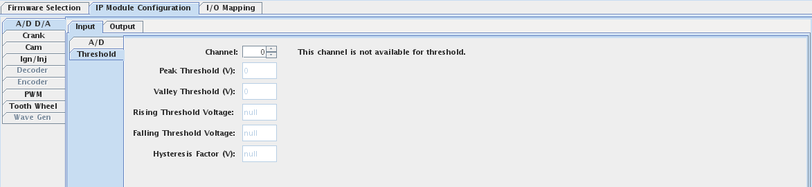
Analog Threshold Settings:
- Channel: Select the analog input channel to apply the thresholds.
- Rising Threshold:Enter the voltage threshold to be applied on the rising edge of the analog input signal. Make sure this
voltage is within the range set in the A/D D/A Settings pane.
- Falling Threshold:Enter the voltage threshold to be applied on the falling edge of the analog input signal. Make sure this
voltage is within the range set in the A/D D/A Settings pane.
- Hysteresis Factor: Enter the hysteresis voltage. This hysteresis factor is used to determine the rising and falling of the
analog input signal. Use the hyseteresis factor for analog input signals with a lot of noise.
|
 |
|
Encoder Settings:
- Channel: Select a Encoder channel for configuration. Up to 32 channels depending on firmware options.
- Pulses Per Revolution:Enter the size of Phase A rising edges.
- Start Angle:Enter in degrees the starting angle of the Encoder channel.
- Z Pulse Width: This is the width of the z-pulse in degrees.
- Z Start: This is the starting angle for the z pulse’s rising edge in degrees.
- Polarity: Encoder signals are transmitted as Active High or Active Low.
The Summary section provides an overview of the channel configuration.
|
 |
|
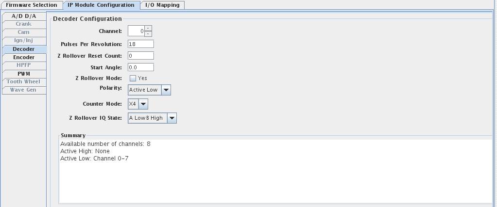
Decoder Settings:
- Channel: Select a Decoder channel for configuration. Up to 32 channels depending on firmware options.
- Pulses Per Revolution:Enter the size of Phase A rising edges.
- Z Rollover Reset Count: Enter the Z counter value for the Decoder channel. If the user wants the Decoder channel counter to begin from a specified value for every Z rollover then the user can specify it in this field.
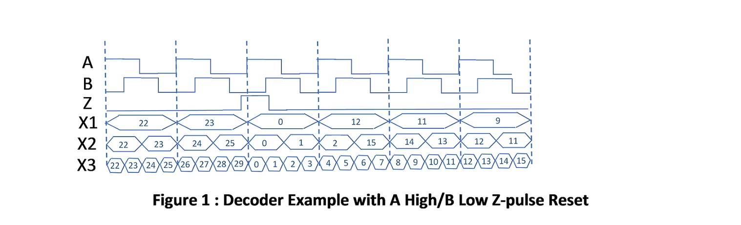
- Start Angle:This parameter is the starting angle of the decoder in degrees. The starting angle of the decoder along with the number of A pulses, and the mode of operation (X1,X2,X4) will define the initial count loaded into the decoder. For example if X4 is used with 36 teeth at an offset of 45 degrees the counter will be loaded with an 18.
- Z Rollover Mode: Select this if you want the Decoder channel to rollover at Z pulse.
- Polarity: Decoder signals are received as Active High or Active Low.
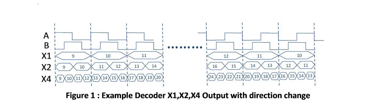
- Counter Mode: Select the counter mode X1, X2 or X4 depending on if you want the counter to be updated on A's rising edge, A's rising and falling edges or updated everytime the Decoder encounters A's or B's rising or falling edges.
- Z Rollover IQ State:This parameter will define on which A/B edge the counter reset will occur. This is also a function of the user defined mode of operation (X1,X2,X4). For example X2 can have the Z-pulse reset occur on either A High/B Low or A Low/B High. It is important to understand that the Z-pulse must span the A/B edge that you expect the reset to occur. If the Z-pulse does not span the desired A/B the decoder will miss the Z-pulse and continue counting. Please see the following example for a proper Z-pulse location.
- Filter Count: Set the filter count to filter out a noisy digital input signal. The filter count is a 8 bit interger with the count reprensting the clock cycles. After a digital input rising or falling edge, the input must remain high/low for greater than the “Filter Count” clock cycles to be counted.
The Summary section provides an overview of the channel configuration.
|
 |
|
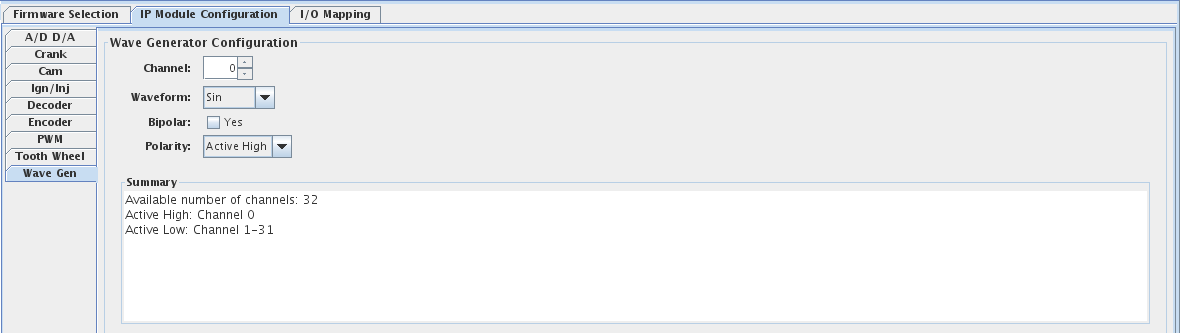
Wave Gen Settings:
- Channel: Select a Wave Gen channel for configuration. Up to 32 channels depending on firmware options
- Waveform: Select the output wave form to be generated which is either Sin, Square, Ramp or Triangle.
- Bipolar: Select yes, if the generated output is desired to range +/-volts
- Polarity: Wave Gen signals are transmitted as Active High or Active Low..
The Summary section provides an overview of the channel configuration.
|
 |
|
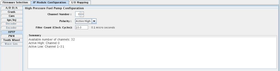
High Pressure Fuel Pump Settings:
- Channel: Select a High Pressure Fuel Pump channel for configuration. Up to 32 channels depending on firmware options
- Polarity: High Pressure Fuel Pump signals are transmitted as Active High or Active Low..
- Filter Count: Set the filter count to filter out a noisy digital input signal. The filter count is a 24 bit interger with the count reprensting the clock cycles. After a digital input rising or falling edge, the input must remain high/low for greater than the “Filter Count” clock cycles to be counted and thus stored in the FIFO.
The Summary section provides an overview of the channel configuration.
|
 |
|
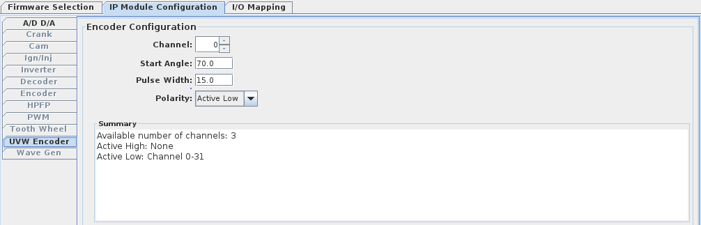
UVW Encoder Settings:
- Channel: Select a UVW Encoder channel for configuration. Up to 32 channels depending on firmware options.
- Start Angle: Enter in degrees the starting angle of the UVW Encoder channel.
- Pulse Width: This is the width of the U V and W Output pulses in degrees.
- Polarity: UVW Encoder signals are transmitted as Active High or Active Low.
The Summary section provides an overview of the channel configuration.
|
 |
|
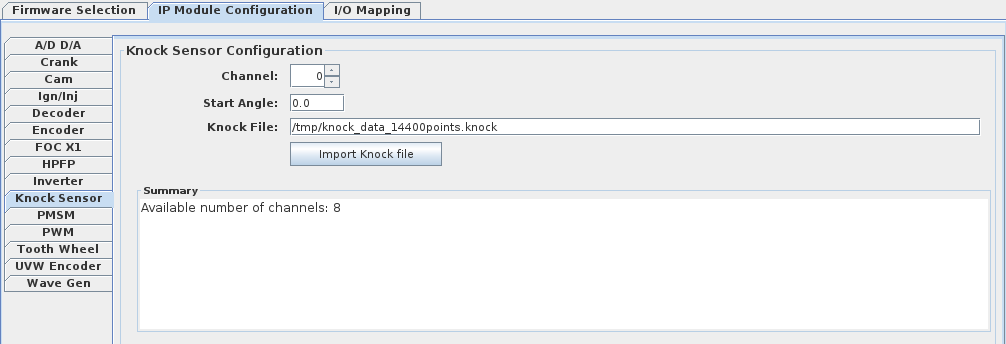
Knock Sensor Settings:
- Channel: Select a Knock Sensor channel for configuration. Up to 8 channels depending on firmware options.
- Start Angle: Enter in degrees the starting angle of the Knock Sensor channel.
- Knock File: Import the knock input file (*.knock). It contains two colums which are comma separated. First column is the angle step and it should be atleast 0.05
degrees. Second column is the voltage in volts. The file can contain a maximum of 16385 values.
The Summary section provides an overview of the channel configuration.
|
 |
|
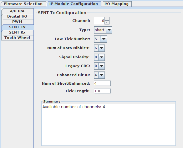
SENT Transmitter Settings:
- Channel: Select the SENT Tx channel for configuration. Up to 8 channels depending on firmware options. It defaults to 0.
- Type: The field type specifies the type of data transmission and takes values 0-Short message format, 1-Enhanced message format and 2-Fast. It defaults to short.
- Low Tick Number: Low tick number signifies number of ticks the signal is low between falling edge and following positive edge and takes values
greater than 5 and less than 11 inclusive.
- Num of Data Nibbles: Number of data nibbles to be transmitted and takes value 1 to 6. Based on the selection here the IO mapping panel for
SENT Tx is reconfigured with the respective number of nibbles nodes.
- Signal Polarity: Signal polarity signifies if to transmit signal as active low or active high and takes value 0 or 1 respectively.
- Legacy CRC: Legacy CRC takes values 0 or 1 and indicates mechanism to calculate the CRC Checksum nibble. CRC checksum is implemented
as a series of shift left by 4 (multiply by 16) followed by a 256 array look-up.
- Enhanced Bit ID: Enhanced bit ID takes values 4 or 8 and indicates if the the SENT IDs used for enhanced message format is a 4 bit ID or a 8 bit ID.
- Num of Short/Enhanced: Number of Short/Enhanced is the number of short/enhanced messages to be transmitted. It takes value 1 to 4 for short type
and 1 to 512 for enhanced type. Based on the selection here, the IO mapping panel for SENT Tx is reconfigured with the respective number of SENT IDs nodes.
- Tick Length: Tick length is the length of the clock tick in microseconds and takes values greater than 1 and less than 990 inclusive.
|
 |
|
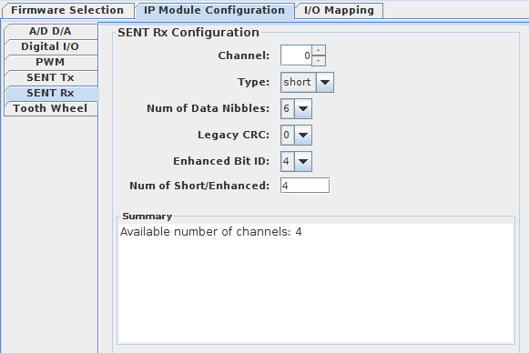
SENT Receiver Settings:
- Channel: Select the SENT Rx channel for configuration. Up to 8 channels depending on firmware options. It defaults to 0.
- Type: The field type specifies the type of data received and takes values 0-Short message format, 1-Enhanced message format and 2-Fast. It defaults to short.
- Num of Data Nibbles: Number of data nibbles to be received and takes value 1 to 6. Based on the selection here the IO mapping panel for
SENT Rx is reconfigured with the respective number of nibbles nodes.
- Legacy CRC: Legacy CRC takes values 0 or 1 and indicates mechanism to calculate the CRC Checksum nibble. CRC checksum is implemented
as a series of shift left by 4 (multiply by 16) followed by a 256 array look-up.
- Enhanced Bit ID: Enhanced bit ID takes values 4 or 8 and indicates if the the SENT IDs used for enhanced message format is a 4 bit ID or a 8 bit ID.
- Num of Short/Enhanced: Number of Short/Enhanced is the number of short/enhanced messages to be received. It takes value 1 to 4 for short type
and 1 to 512 for enhanced type. Based on the selection here, the IO mapping panel for SENT Rx is reconfigured with the respective number of SENT IDs nodes.
|
 |
|
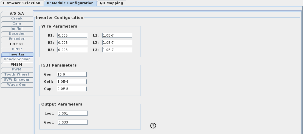
| Inverter Settings:
Wire Parameters
- R1: This is the resistance of the wire between the battery and A IGBT switch. It defaults to 5e-3 ohms.
- R2: This is the resistance of the wire between A IGBT switch and B IGBT switch. It defaults to 5e-3 ohms.
- R3: This is the resistance of the wire between B IGBT switch and C IGBT switch. It defaults to 5e-3 ohms.
- L1: This is the inductance of the wire between the battery and A IGBT switch. It defaults to 100e-9 mH.
- L2: This is the inductance of the wire between the A IGBT switch and B IGBT switch. It defaults to 100e-9 mH.
- L3: This is the inductance of the wire between the B IGBT switch and C IGBT switch. It defaults to 100e-9 mH.
IGBT Parameters
- Gon: This represents the admittance for the IGBT switch in the ON state. It defaults to 100.
- Goff: This represents the admittance for the IGBT switch in the OFF state. It defaults to 1e-4.
- Cap: This represents the capacitance for the IGBT switches. It defaults to 20e-9.
Output Parameters
- Lout: This represents an approximation of the inductance for the inverter’s load. It defaults to 1e-3.
- Gout: This represents an approximation of the admittance for the Inverter’s load. It defaults to 0.033.
The help icon has the circuit diagram for the Inverter.
|
 |
|
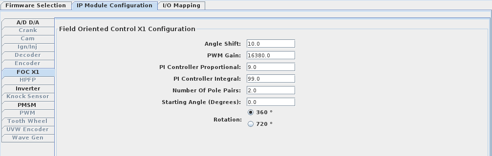
Field Oriented Control X1 Settings:
- Angle Shift: This value shifts the angle increment input to extend the range of acceptable increment angles inside of the
3-phase PWM logic. Thus a smaller shift will support the slower RPM's and a larger shift will support very large RPM's.
The maximum acceptable value is 12 and it defaults to 10.
- PWM Gain: The PWM gain tries to have its internally generated triangular wave to match the input current error (after the PI controller) from the PMSM. It defaults to 16380.
- PI Controller Proportional: PI Controller proportional is the proportional gain of the PI Controller. The PI Controller's purpose is to filter the angular speed error between the user desired speed and the instantaneous speed of the PMSM ensuring the correct steady state value is achieved as required by the algorithm. It defaults to 9.
- PI Controller Integral: PI Controller Integral is the integral gain of the PI Controller. he PI Controller's purpose is to filter the angular speed error between the user desired speed and the
instantaneous speed of the PMSM ensuring the correct steady state value is achieved as required by the algorithm. It defaults to 99.
- Number of Pole Pairs: Number of pole pairs in the PMSM Model. It defaults to 2.
|
 |
|
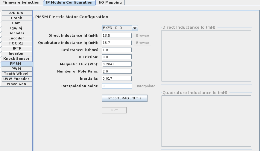
PMSM Electric Motor Settings:
- Resistance (Ohms): This is the resistance of the stator windings in the PMSM Model. It defaults to 1.
- B Friction: B Friction in the PMSM Model. It defaults to 0.
- Magnetic Flux (Wb): Magnetic flux in Webers linking the stator windings of the PMSM Model. It defaults to 0.2041 Wb.
- Number of Pole Pairs: Number of pole pairs in the PMSM Model. It defaults to 2.
- Inertia Ja: Inertia of the PMSM Model. It defaults to 0.0170.
Fixed LDLQ
- Direct Inductance ld (mH): Direct Inductance in the stator of the PMSM Model. It defaults to 16.5 mH.
- Quadrature Inductance lq (mH): Quadrature Inductance in the stator of the PMSM Model. It defaults to 18.7 mH.
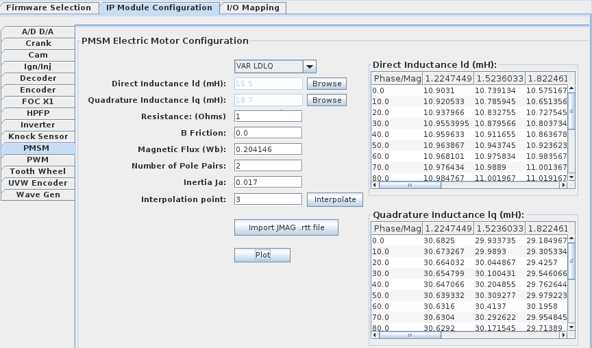
Variable LDLQ
- Direct Inductance ld (mH): Import a (*.dat or *.txt) file that contains the LD values using the Browse button.
The file contains magnitude in the first row, phase in the second row and then followed by the LD matrix.
-
Eg: Contents of ld.txt
1, 2, 3, 4
0, 45, 90
16, 15, 14, 13
16, 15, 14, 13
16, 15, 14, 13
- Quadrature Inductance lq (mH): Import a (*.dat or *.txt) file that contains the LQ values using the Browse button.
The file contains magnitude in the first row, phase in the second row and then followed by the LQ matrix.
-
Eg: Contents of lq.txt
1, 2, 3, 4
0, 45, 90
18, 17, 16, 15
18, 17, 16, 15
18, 17, 16, 15
- Interpolation point: Specify an integer value to interpolate the LD/LQ matrix.
Import the JMAG (.rtt) file using the Import button and see the above fields updated in the GUI based on the values for them in the file.
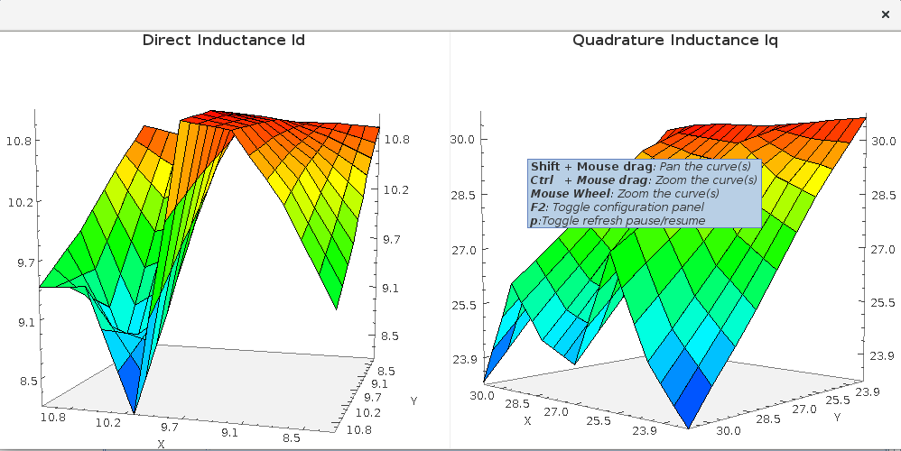
Plot the LD/LQ matrix using the Plot button for a 3D view.
|
 |
 |
 |
|
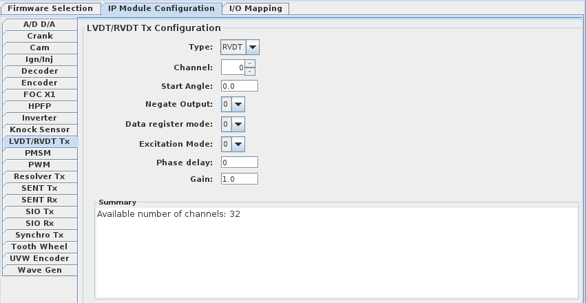
LVDT/RVDT Tx Settings:
- Type: Type indicates if the IP functions as RVDT or LVDT. It defaults to RVDT mode.
- Channel: Select the LVDT/RVDT Tx channel for configuration. Up to 8 channels depending on firmware options. It defaults to 0.
- Start Angle: Internal Excitation Starting Angle of the LVDT/RVDT Tx IP Core Channel rotation. It takes values 0 - 360 in degrees and defaults to 0 degree.
- Negate Output: Negate output negates the three output ports vs1, vs2 and excitation out. This is accomplised by using a three bit parameter whereby LSB bit negates vs1, second bit negates vs2, MSB negates excitation.
- Data register mode: The data_register_mode takes value 0 for signal input and 1 for register input.
- Excitation mode: Excitation Mode takes values 0 or 1 (0= internally generated excitation, 1= externally generated excitation applied through the input port) and it defaults to 0.
- Phase Delay: Phase delay is delay for vs1 and vs2 in 100ns increments up to max of 50. It defaults to 0.
- Gain: Gain is used to scale the output relative to the input. It takes value 0 to 31 and has nine fractional bits. It defaults to 1.
The Summary section provides an overview of the channel configuration.
|
 |
|
Resolver Tx Settings:
- Channel: Select the Resolver Tx channel for configuration. Up to 32 channels depending on firmware options. It defaults to 0.
- Start Angle: Internal Excitation Starting Angle of the Resolver Tx IP Core Channel rotation. It takes values 0 - rotation in degrees and defaults to 0 degree.
- Negate Output: Negate output negates the three outputs cos, sin and excitation out. This is accomplised by using a three bit parameter whereby LSB negates cos, middle bit negates sin and the MSB negates excitation out.
- Data register mode: Data Register Mode takes values 0 or 1(0-signal input from port, 1-signal input from register) and defaults to 0.
- Excitation mode: Excitation Mode takes values 0 or 1 (0= internally generated excitation, 1= externally generated excitation applied through the input port) and it defaults to 0.
- Rotation: Rotation of the Excitation input of the Resolver Tx IP Core Channel. It takes values 360 or 720 degrees and defaults to 360 degree.
- Phase Delay: Phase delay is delay for cos and sin in 100ns increments up to max of 50. It defaults to 0.
- Gain: Gain is used to scale the output relative to the input. It takes value 0 to 31 and has nine fractional bits. It defaults to 1.
The Summary section provides an overview of the channel configuration.
|
 |
|
Synchro Tx Settings:
- Channel: Select the Synchro Tx channel for configuration. Up to 32 channels depending on firmware options. It defaults to 0.
- Start Angle: Internal Excitation Starting Angle of the Synchro Tx IP Core Channel rotation. It takes values 0 - rotation in degrees and defaults to 0 degree.
- Negate Output: Negate output negates the four output ports a, b, c and excitation out. This is accomplised by using a four bit parameter whereby LSB bit negates a, second bit negates b, third bit negates c and MSB negates excitation out.
- Data register mode: Data Register Mode takes values 0 or 1(0-signal input from port, 1-signal input from register) and defaults to 0.
- Excitation mode: Excitation Mode takes values 0 or 1 (0= internally generated excitation, 1= externally generated excitation applied through the input port) and it defaults to 0.
- Rotation: Rotation of the Excitation input of the Synchro Tx IP Core Channel. It takes values 360 or 720 degrees and defaults to 360 degree.
- Phase Delay: Phase delay is delay for a, b and c in 100ns increments up to max of 50. It defaults to 0.
- Gain: Gain is used to scale the output relative to the input. It takes value 0 to 31 and has nine fractional bits. It defaults to 1.
The Summary section provides an overview of the channel configuration.
|
 |
|
SIO Tx Settings:
- Channel: Select the SIO Tx channel for configuration. Up to 4 channels depending on firmware options. It defaults to 0.
- Tx mode: Tx mode is the mode of transmission. It takes value 0-RCIM or 1-Immediate transfer test mode. It defaults to 1.
- SIO mode: SIO mode identifies Fast SIO or Standard SIO. It takes value 0-Fast SIO or 1-Standard SIO.
- Word Size: Word size is the number of bits in a word. It takes value 4, 8, 16 or 32.
- PLL Frequency: Frequency of the PLL in units of MHz. It takes value 4.5 to 20 in increments of 0.5 MHz for Fast SIO and takes value 0.5 to 4.5 in 0.0625 MHz increments.
- SYNC Start: Parameter to offset the SYNCn from the RCIM's rising edge. It takes values in units of clock cycles. The min value is 8 to (2^20-1).
- SYNC Width: Parameter to specify the width of SYNCn pulse. It takes values in units of clock cycles. It takes value 8 to (2^20-1).
- Enable Delay: Parameter to offset the enable from the RCIM's rising edge. It takes values in units of clock cycles. It takes value greater than Sync Start + Sync Width + 4 with a min of 20 to max of (2^20-1).
- RCIM Pulses: This is the number of RCIM pulses to be expected between every transmission of the data. It takes value 0 to 15 corresponding to 1 to 16 RCIM pulses.
- NFrames between SYNCn: This is the number of data frames between each SYNCn pulse.
- CED Invert: This is the one-hot invert for the C, E and D lines. It takes value 0 to 7. This is accomplished by using a three bit parameter whereby LSB bit negates D, second bit negates E and
MSB negates C. It defaults to 0.
- RCIM Invert: This is the invert for the RCIM. It takes value 0 or 1 and defaults to 0.
- SYNC Invert: This is the invert for the SYNC. It takes value 0 or 1 and defaults to 0.
- Endian: This is used for controlling if the data is written LSB or MSB first. It takes value 0 or 1. If 1, first bit written is the LSB of the word written to the RAM. If 1, first bit written is the MSB of the word written to the RAM.
The Summary section provides an overview of the channel configuration.
|
 |
|
SIO Rx Settings:
- Channel: Select the SIO Rx channel for configuration. Up to 4 channels depending on firmware options. It defaults to 0.
- Word Size: Word size is the number of bits in a word. It takes value 4,8,16 or 32.
- SIO mode: SIO mode identifies Fast SIO or Standard SIO. It takes value 0-Fast SIO or 1-Standard SIO.
- CED Invert: This is the one-hot invert for the C, E and D lines. It takes value 0 to 7. This is accomplished by using a three bit parameter whereby LSB bit negates D, second bit negates E and
MSB negates C. It defaults to 0.
- Endian: This is used for controlling if the data is writted LSB or MSB first. It takes value 0 or 1. If 1, first bit received in the data stream from the serial interface will be the LSB of the word in the RAM. If 1, first bit
received in the data stream from the serial interface will be the MSB of the word in the RAM.
The Summary section provides an overview of the channel configuration.
|
 |
|
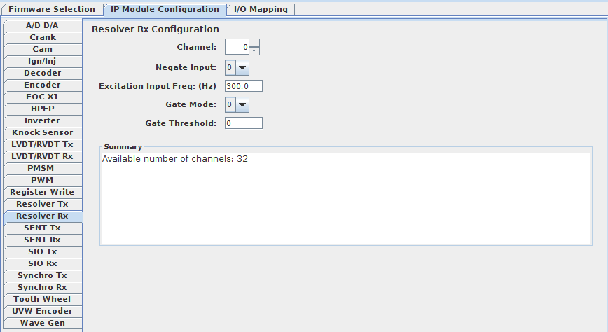
Resolver Rx Settings:
- Channel: Select the Resolver Rx channel for configuration. Up to 32 channels depending on firmware options. It defaults to 0.
- Negate Input: negates the three input signals cos, sin and excitation input. This is accomplised by using a three bit one-hot parameter whereby LSB bit negates
cos, second bit negates sin and MSB negates excitation input. For example: selecting a value of 4(100) in the drop down list negates the excitation signal.
- Excitation Frequency: The external excitation frequency input aids in the selection of the clock for the FIR filter.
If the frequency of the External Input Excitation is in the range of 300-800 Hz then 2.44 Khz clock will be selected.
If the frequency of the External Input Excitation is in the range of 801-2000 Hz then 9.77 Khz clock will be selected.
If the frequency of the External Input Excitation is in the range of 2001-8000 Hz then 19.53 Khz clock will be selected.
If the frequency of the External Input Excitation is in the range of 8001-13000 Hz then 78.125 Khz clock will be selected.
- Gate Mode: Gate mode enables the zeroing of lower bits of the angular position prior to velocity computation. It takes value 0 or 1 and defaults to 0.
- Gate Threshold: Gate threshold takes value 6 to 20 and determines how many lower bits of the angular position will be zeroed. It defaults to 0.
The Summary section provides an overview of the channel configuration.
|
 |
|
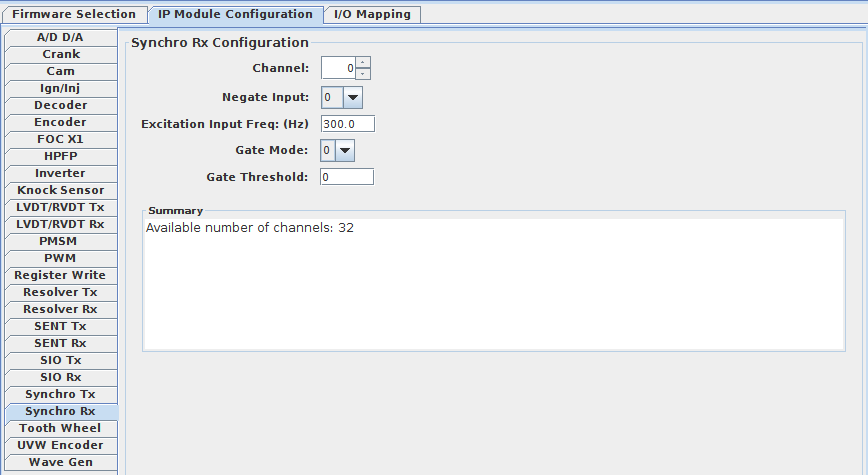
Synchro Rx Settings:
- Channel: Select the Synchro Rx channel for configuration. Up to 32 channels depending on firmware options. It defaults to 0.
- Negate Input: negate_input negates the four input signals a, b, c and excitation. This is accomplised by using a four bit one-hot parameter whereby
LSB bit negates a, second bit negates b, third bit negates c and MSB negates excitation input. For example: selecting a value of 5(0101) in the drop down list
negates a and c signals.
- Excitation Frequency: The external excitation frequency input aids in the selection of the clock for the FIR filter.
If the frequency of the External Input Excitation is in the range of 300-800 Hz then 2.44 Khz clock will be selected.
If the frequency of the External Input Excitation is in the range of 801-2000 Hz then 9.77 Khz clock will be selected.
If the frequency of the External Input Excitation is in the range of 2001-8000 Hz then 19.53 Khz clock will be selected.
If the frequency of the External Input Excitation is in the range of 8001-13000 Hz then 78.125 Khz clock will be selected.
- Gate Mode: Gate mode enables the zeroing of lower bits of the angular position prior to velocity computation. It takes value 0 or 1 and defaults to 0.
- Gate Threshold: Gate threshold takes value 6 to 20 and determines how many lower bits of the angular position will be zeroed. It defaults to 0.
The Summary section provides an overview of the channel configuration.
|
 |
|
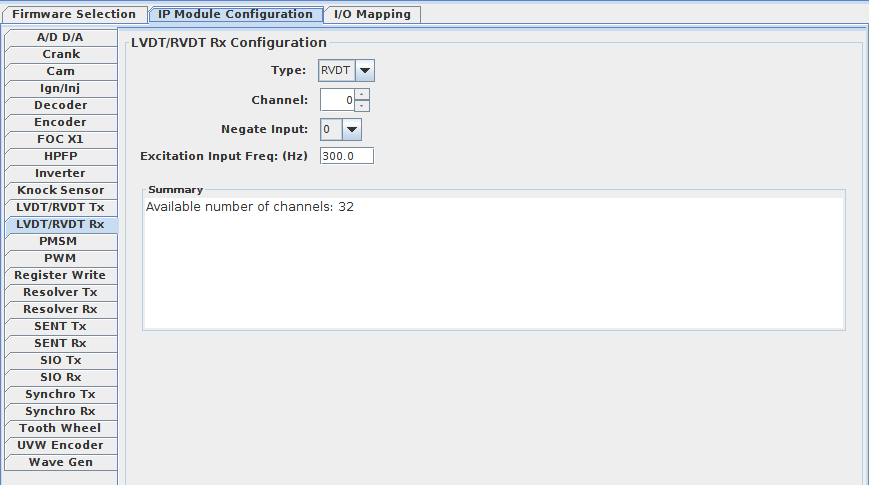
LVDT/RVDT Rx Settings:
- Type: Type indicates if the IP functions as RVDT or LVDT. It defaults to RVDT mode.
- Channel: Select the LVDT/RVDT Rx channel for configuration. Up to 32 channels depending on firmware options. It defaults to 0.
- Negate Input: negate_input negates the four input ports vs1, vs2, am and input excitation. This is accomplised by using a four bit one-hot parameter whereby
LSB bit negates vs1, second bit negates vs2, third bit negates am and MSB negates excitation input.
For example: selecting a value of 5(0101) in the drop down list negates vs1 and am signals.
- Excitation Frequency: The external excitation frequency input aids in the selection of the clock for the FIR filter.
If the frequency of the External Input Excitation is in the range of 300-800 Hz then 2.44 Khz clock will be selected.
If the frequency of the External Input Excitation is in the range of 801-2000 Hz then 9.77 Khz clock will be selected.
If the frequency of the External Input Excitation is in the range of 2001-8000 Hz then 19.53 Khz clock will be selected.
If the frequency of the External Input Excitation is in the range of 8001-13000 Hz then 78.125 Khz clock will be selected.
The Summary section provides an overview of the channel configuration.
|
 |
|
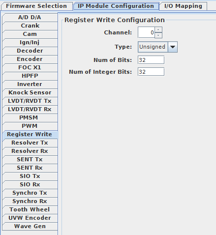
Register Write Settings:
- Channel: Select the Register Write channel for configuration. Up to 128 channels depending on firmware options. It defaults to 0.
- Type: Type respresents the data type of the number and it takes value 0 for unsigned and 1 for signed.
- Num of Bits: Num of bits is the total number of bits used to represent the fixed-point number and it takes value 1 to 32.
- Num of Integer Bits: Num of Integer bits is the total number of integer bits used to represent the fixed-point number and takes value 0 to 32
it's value should be less than the number of bits specified.
|
 |
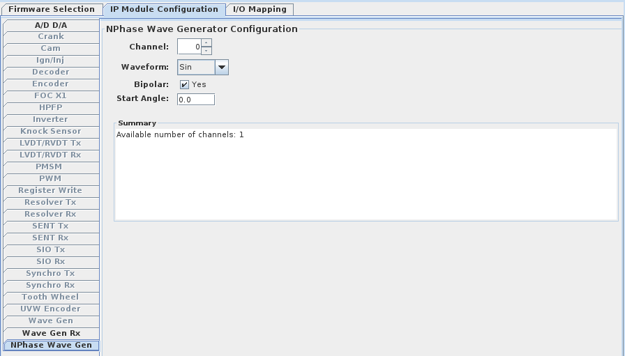
N-Phase Wave Gen Settings:
- Channel: Select a N-Phase Wave Gen channel for configuration. Up to 32 channels depending on firmware options. It defaults to 0.
- Waveform: Select the output wave form to be generated which is either Sin, Square, Ramp or Triangle.
- Bipolar: Select yes, if the generated output is desired to range +/-volts
- Start Angle: Start angle of the main cos(x) and sin(x) cordic. It takes value -360 to +360 degrees.
The Summary section provides an overview of the channel configuration.
|
 |
|
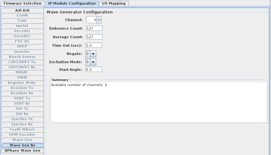
Wave Gen Rx Settings:
- Channel: Select a Wave Gen Rx channel for configuration. Up to 32 channels depending on firmware options. It defaults to 0.
- Debounce count: Filter count used in the debouncing circuit. It takes value 0 to 127.
- Average count: Depth of the FIFO. It takes value 0 to 127.
- Time out(sec): Dead limit specifies the number of clock cycles after a high or low whereby the output
will assume dead low or dead high. It is calculated by multiplying timeout in seconds by 100MHz.
- Negate: Negate takes value 0 or 1, the I/Q output will be negated when this is set to 1, the phase is rotated by 180 degrees.
- Excitation Mode: Excitation mode takes value 0 or 1, when set to 0 the carrier is internally generated and
when set to 1 it is external input-sin and cos.
- Start Angle: Start angle of the carrier. It takes value -360 to +360 degrees.
The Summary section provides an overview of the channel configuration.
|
 |
|
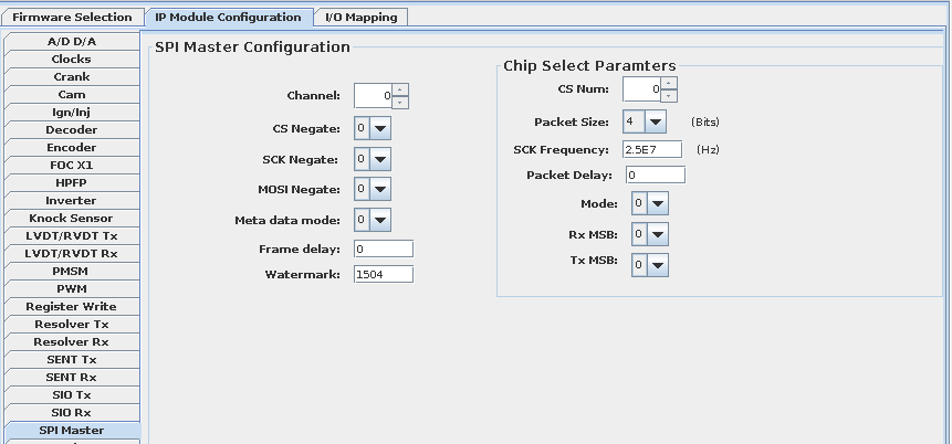
SPI Master Settings:
- Channel: Select a SPI Master channel for configuration. Up to 8 channels depending on firmware options. It defaults to 0.
- CS Negate: CS Negate takes value 0 or 1, a value of 1 indicates that the CS is negated.
- SCK Negate: SCK Negate takes value 0 or 1, a value of 1 indicates that the SCK is negated.
- MOSI Negate: MOSI Negate takes value 0 or 1, a value of 1 indicates that the MOSI is negated.
- Meta data mode: Meta data mode takes value 0 or 1, a value of 1 will record the meta data information for the packets received in the FIFO.
Enabling this mode will add two additional words for each command executed. The first word contains the command and the second word contains number
of packets expected for the command from the slave device.
- Frame delay: Frame delay is the amount of IP Clock cycles in 10ns delayed between each frame of packets. It takes a 32 bit integer value.
- Watermark: Watermark signifies the threshold value that will trigger the watermark flag if the FIFO reaches that many used words.
It takes a maximum value of 1504(0x5E0).
- CS Num: Each SPI Master channel can communicate with upto 6 slave device and CS parameters can be independently programmed
using this CS Num Spinner.
- Packet Size: Packet Size determines the number of bits each packet will carry. It takes value 4 to 32 in increments of 4.
- SCK Frequency: SCK Frequency is the frequency in Hertz of the SCK output line and takes value upto 25MHz.
- Packet Delay: Packet Delay determines the amount of time between two consecutive packets being sent on the CS and is based on SCK Clk cycles.
By default there is a minimum delay of 4 SCK cycles.
- Mode: Mode identifies the polarity and phase mode the SCK functions in for the specific CS line. It is a 2 bit parameter and
takes value 0 to 3. It is a one-hot parameter where in LSB bit is the CPHA phase bit for spi sck control, when set to 1 the phase is offset
to the 2nd edge, and when set to first edge when set to 0. The MSB bit is the CPOL bit where the SCK is idle HI when set to 1 and idle LO when set to 0.
- Rx MSB: Rx MSB controls receiving bit order. If 1 then the first received bit is stored as the MSB, if 0 then the first received word is
stored as the LSB.
- Tx MSB: Tx MSB controls transmission bit order. If 1 then the MSB is transmitted first, if 0 then LSB is transmitted first.
The Summary section provides an overview of the channel configuration.
|
 |
|
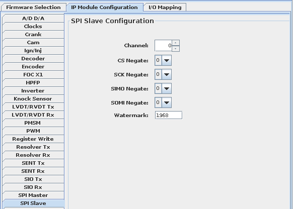
SPI Slave Settings:
- Channel: Select a SPI Slave channel for configuration. Up to 8 channels depending on firmware options. It defaults to 0.
- CS Negate: CS Negate takes value 0 or 1, a value of 1 indicates that the CS is negated.
- SCK Negate: SCK Negate takes value 0 or 1, a value of 1 indicates that the SCK is negated.
- SIMO Negate: SIMO Negate takes value 0 or 1, a value of 1 indicates that the SIMO is negated.
- SOMI Negate: SOMI Negate takes value 0 or 1, a value of 1 indicates that the SOMI is negated.
- Watermark: Watermark signifies the threshold value that will trigger the watermark flag if the FIFO reaches that many used words.
It takes a maximum value of 1968(0x7B0).
The Summary section provides an overview of the channel configuration.
|
 |
|
| Wheel Speed Sensor Settings:
Wheel setup
- Channel: Select a Wheel Speed Sensor channel for configuration. Up to 32 channels depending on firmware options. It defaults to 0.
- Protocol: Select the protocol to be used from the drop-down 0-AK, 1-PWM, 2-DF10 and 3-DF11.
- Variant: Variant identifies the variant for the protocol selected. It takes value 0 or 1, DF10: 0-No variant and 1-Rot-Dir variant, DF11-N/A, PWM: 0-No variant and 1-High Res variant, AK: 0-No variant and 1-High Res variant.
- Zeroth polarity: Zeroth Polarity indicates the polarity of the magnet at Index 0. It takes value 0 or 1, 0-North and 1-South.
- Voltage mode: Voltage mode indicates 5V or 12V.
- Total magnet: Total Magnet indicates the total number of magnets in the wheel and takes an even number from 2 to 128.
- Calibration magnet size: Calibration Magnet Size indicates how many poles plus boundaries need to be seen from the wheel before outputting pulses after startup and/or faults.
- Start magnet index: Start Magnet Index indicates the index of the magnet that the start angle resides in and is 0's based.
- Start angle: Start angle indicates the angle position of wheel on startup in degrees. It takes value 0 to 360 degrees.
Boundaries and Poles setup
- Boundaries and Poles: Import a file of max entries 256 where alternate indices has boundaries and poles in degrees, starting with boundary at 0 degrees and every pole
and boundary after should sequentially increase. It takes value 0 to 360 degrees. On the FPGA the center of the magnet will be considered it's pole and the crossing from a North to
South side of a dipole is considered a boundary.The number of boundaries loaded should always be equal to the number of poles loaded as well and this number should be equal to the total magnet.
AK protocol parameters
- Tp Half: Tp Half defines the time-base(tp) value for the AK protocol based on steps of 10Mhz periods(0.1us).
- Tpssd: Tpssd defines the length of time in steps of 10Mhz periods(0.1us) that represents the amount of forced wait time between a truncated standstill pulse and a high resolution pulse.
- Bit control: Bit control defines which values will populate each data bit in the AK transmit packet. Each data bit in the AK packet data is identified by a 3 bit mask and
hence (9x3)27 bit mask to represet a 9 bit packet data. The 3 bit mask takes value 0 to 7, 0-Software[x],1-Direction,2-Direction Valid,3-hres_index[2],4-hres_index[1],5-hres_index[0],
6-standstill,7-Parity.Eg: If bitcontrol is set to 111001110101100011010001000(d'121292424) then the 9 bit AK packet data will represent Parity,Direction,standstill,hres_index[0],hres_index[1].hres_index[2],
Direction Valid,Direction,Software[x] MSB to LSB.
- High freq hysteresis: High freq hysteresis is used to identify which speed mode of operation to use for pulse outputs. It takes value in Hertz and defaults to 1000Hz(1ms).
- Low freq hysteresis: Low freq hysteresis is used to identify which speed mode of operation to use for pulse outputs. It takes value in Hertz and defaults to 900Hz(1.1111ms).
- Forced low time: Forced low time indicates how long the signal pulses must be forced to a LO values between the pulses in units of 10Mhz periods(0.1us).
- High resolution offset: High resolution offset value represents the amount of degrees above and below each pole where the high resolution pulses will be generated.
Eg: Typically the magnet profile is uniform, so if boundaries would exist at 0 degrees and 3 degrees then pole would be at 1.5 degrees. For the high resolution pulses
to be perfectly between poles and boundaries at 0.75 degrees and 2.25 degrees, the offset need to be set to 0.75 degrees since 1.5 degrees +/- 0.75 degrees yields the desired values.
- Standstill sensitivity: Standstill sensitivity defines the amount of time in 10Mhz periods(0.1us) for no pulse to be seen to enact a standstill pulse.
PWM protocol parameters
- Forward pulse width: Forward pulse width defines the pulse width in 10Mhz period steps(0.1us) for pulse output when the direction is forward.
- Reverse pulse width: Reverse pulse width defines the pulse width in 10Mhz period steps(0.1us) for pulse output when the direction is reverse.
- Standstill pulse width: Standstill pulse width defines the pulse width in 10Mhz period steps(0.1us) for pulse output when a standstill call occurs.
- High freq hysteresis: High freq hysteresis is used to identify which speed mode of operation to use for pulse outputs. It takes value in Hertz and defaults to 1000Hz(1ms).
- Low freq hysteresis: Low freq hysteresis is used to identify which speed mode of operation to use for pulse outputs. It takes value in Hertz and defaults to 900Hz(1.1111ms).
- Forced low time: Forced low time indicates how long the signal pulses must be forced to a LO values between the pulses in units of 10Mhz periods(0.1us).
- High resolution offset: High resolution offset value represents the amount of degrees above and below each pole where the high resolution pulses will be generated.
Eg: Typically the magnet profile is uniform, so if boundaries would exist at 0 degrees and 3 degrees then pole would be at 1.5 degrees. For the high resolution pulses
to be perfectly between poles and boundaries at 0.75 degrees and 2.25 degrees, the offset need to be set to 0.75 degrees since 1.5 degrees +/- 0.75 degrees yields the desired values.
- Highspeed pulse width: Highspeed pulse width defines the pulse width in 10Mhz period steps(0.1us) for pulse output for both directions whenever the speed mode defined by frequency hysteresis is high speed.
- Standstill sensitivity: standstill sensitivity defines the amount of time in 10Mhz periods(0.1us) for no pulse to be seen to enact a standstill pulse.
DF10 protocol parameters
- Pulse width: Pulse width defines the pulse width in 10Mhz period steps(0.1us) for the extra 28mA pulse output when the direction is in reverse and the Rot-Dir Protocol variant is being used.
- Pole inversion: Pole inversion inverts the polarity of the wheel's current magnet. It takes value 0 or 1 and a value of 1 inverts the polarity of the current magnet.
DF11 protocol parameters
- Time base: Time base defines the pulse width in 10Mhz period steps(0.1us) for the reference t0 used by other pulse widths. Default is typically 45us.
- Very low magnet pulse width: Very low magnet pulse width defines the pulse width in t0 period steps for pulses when the df11_strength is set to very low mode.
Defined pulse width is (very_low_magnet_width + 1)*t0. Default is 1t0 so very_low_magnet_width value passed in is 0.
- Normal magnet forward pulse width: Normal magnet forward pulse width defines the pulse width in t0 period steps for pulses when the df11_strength is set to normal mode and wheel direction is forward.
Defined pulse width is (normal_magnet_forward_width + 1)*t0. Default is 4t0 so normal_magnet_forward_width value passed in is 3.
- Normal magnet reverse pulse width: Normal magnet reverse pulse width defines the pulse width in t0 period steps for pulses when the df11_strength is set to normal mode and wheel direction is reverse.
Defined pulse width is (normal_magnet_reverse_width + 1)*t0. Default is 2t0 so normal_magnet_reverse_width value passed in is 1.
- High magnet forward pulse width: high magnet forward pulse width defines the pulse width in t0 period steps for pulses when the df11_strength is set to high mode and wheel direction is forward.
Defined pulse width is (high_magnet_forward_width + 1)*t0. Default is 16t0 so high_magnet_forward_width value passed in is 15.
- High magnet reverse pulse width: High magnet reverse pulse width defines the pulse width in t0 period steps for pulses when the df11_strength is set to high mode and wheel direction is reverse.
Defined pulse width is (high_magnet_reverse_width + 1)*t0. Default is 8t0 so high_magnet_reverse_width value passed in is 7.
- Standstill pulse width: Standstill pulse width defines the pulse width in t0 period steps for pulses when a standstill pulse is initiated. Defined pulse width is (standstill_pulse_width + 1)*t0.
Default is 32t0 so standstill_pulse_width value passed in is 31.
- Standstill sensitivity: Standstill sensitivity defines the amount of time in 10Mhz periods(0.1us) for no pulse to be seen to enact a standstill pulse.
|
 |
|
|
| I/O Mapping > Notes:
Map an input and an output RTDB variable to the FPGA card for the IO Task to run. Without
these mappings the FPGA Card IO Task does not initialize and will not execute.
|
|
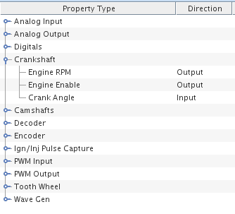
I/O Mapping > Crankshaft:
- Engine RPM: Output from a model or script. The Engine RPM is an input the FPGA.
- Engine Enable: Boolean to enable the Engine FPGA module. When engine Engine Enable is set to 0 the
Engine FPGA module is in the reset state. Engine Enable is an input to the FPGA.
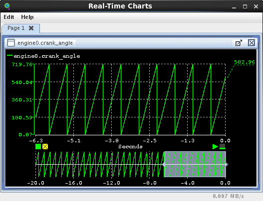
- Crank Angle: Input from the FPGA measure in °CA. Crank Angle is the internal crank angle in the FPGA.
The Crank Angle range is from 0 to 360°/720°. Example Crank Angle waveform is shown below.
|
 |
|
|
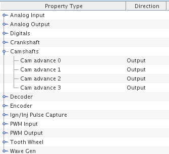
I/O Mapping > Camshafts:
- Cam advance angle 0-3: Cam advance angle, specified in the range of [-60 +60]°. Negative angles indicate delay.
|
 |
|
|
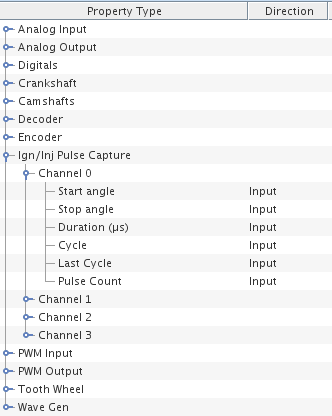
I/O Mapping > Ign/Inj Pulse Capture:
Up to 8 Ignition or Injection pulse information are captured and store in the following mapping variables.
- Start angle:An array of 8 doubles will store the start crank angle (°) of the pulse capture. The captured angle is offset by the cylinder TDC.
For example, if the TDC is set to 20 deg CA then the capture start angle displayed will be (capturedCA - cylinder TDC) i.e. (capturedCA - 20).
- Stop angle:An array of 8 doubles will store the stop crank angle (°) of the pulse capture. The captured angle is offset by the cylinder TDC.
- Duration:An array of 8 doubles will store the energized duration of the input pulse, specified in µs.
- Cycle: Engine cycle count, incremented by +1 for forward and reverse rotation when the Crank Angle passes through the Window Start Crank Angle.
This mapping is an array of 8 doubles and identifies the cycle when the input signal is captured. Specified in the [0 255] range.
- Last Cycle: Incremented for each rotation of the crank.Specified in the [0 255] range.
- Pulse Count: Acquired pulse count, incremented for each pulse detected during the window. Specified in the [0 8] range.
|
 |
|
|
I/O Mapping > Digitals:
The number of available general purpose DIO channels depends on the firmware.
- Group X: Controls whether the group bits are Digital Inputs (default) or Digital Outputs. To change the group type to Digital Output, click Input and select Output from the list.
- Bits Y-Z: Individual bits within the group.
|
 |
|
|
I/O Mapping > Analog Output:
- Channel 0-15: Analog output channels.
|
 |
|
|
I/O Mapping > Analog Input:
- Channel 0-15: Analog input channels.
|
 |
|
|
I/O Mapping > PWM Output:
- Specify the following options for the PWM output channels:
- Frequency (Hz): PWM signal frequency, expressed in Hz.
- Duty Cycle (%): PWM signal duty cycle, expressed as a percentage.
- One Shot Count: Number of periods of specified PWM signal to be transmitted as a single burst.
Only applicable if the option has been enabled in the PWM Configuration pane.
- Constant Pulse Width (µSec): When this field is non zero, the duty cycle is calculated by the I/O task to maintain the pulse width constant when the frequency is changed.
I.e. duty_cycle = pulse_width X 10-6 X frequency X 100. The constant pulse width is expressed in µseconds.
|
 |
|
|
I/O Mapping > PWM Input: Upto 16 channels are captured and the following information is stored:
- Frequency (Hz): PWM signal frequency, expressed in Hz.
- Duty Cycle (%): PWM signal duty cycle, expressed as a percentage.
- Pulse Count: Number of pulses observed in a SimWB frame.
|
 |
|
|
I/O Mapping > Tooth Wheel:
- rpm: RPM as an analog output (AO) in the [-100000, +100000] range, with a resolution of 0.01 RPM. Negative RPM indicates the tooth is moving in the reverse direction.
- angle: Wheel angle, specified in the [0 360]° range..
|
 |
|
|
I/O Mapping > Encoder:
- rpm: Output from a model or script. The Encoder RPM is an input the FPGA.. Negative RPM indicates the tooth is moving in the reverse direction.
- angle: Input from the FPGA measure in °CA. Crank Angle is the internal crank angle in the FPGA.
The Crank Angle range is from 0 to 360°/720°.
|
 |
|
|
I/O Mapping > Decoder:
- Decoder Count: Count value which changes whenever respective edges are detected based on the configured counter mode - X1, X2 or X4.
- Decoder Angle: Decoder Angle, specified in the [0 360]° or [0 720]° range respective to the counter mode set.
- Decoder RPM: Decoder RPM is the frequency with direction output estimate to Angular Decoder.
|
 |
|
|
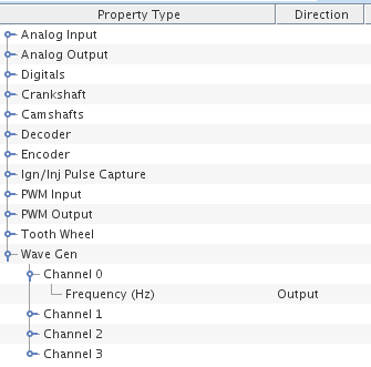
I/O Mapping > Wave Gen:
- Frequency (Hz): Frequency as an analog output (AO) is the phase increment of the IP Core Channel in Hertz. .
|
 |
|
|
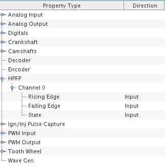
I/O Mapping > High Pressure Fuel Pump:
- Rising Edge (Degree): High Pressure Fuel Pump Angle, specified in the [0 360]° or [0 720]° range respective to the digital input.
- Rising Edge (Degree): High Pressure Fuel Pump Angle, specified in the [0 360]° or [0 720]° range respective to the digital input.
- State: Indicates active or not. Value 1 indicates that HPFP saw a rising edge and the corresponding angle will be in the rising edge. Value 0 indicates that HPFP saw a falling edge and the corresponding angle will be in the falling edge.
|
 |
|
|
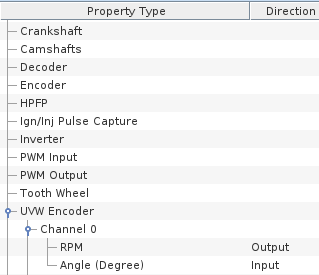
I/O Mapping > UVW Encoder:
- RPM: Output from a model or script. The UVW Encoder RPM is an input the FPGA.. Negative RPM indicates the tooth is moving in the reverse direction.
- Angle: Input from the FPGA measure in °CA. Crank Angle is the internal crank angle in the FPGA.
The Crank Angle range is from 0 to 360°/720°.
|
 |
|
|
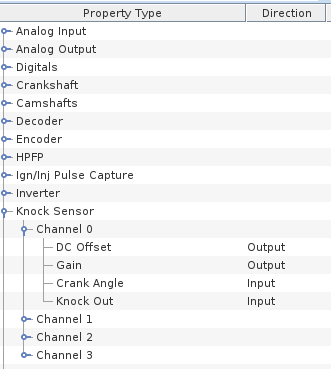
I/O Mapping > Knock Sensor:
- DC Offset: Input a value in volts. This value is added to the knock signal to cause a positive or negative voltage offset. The value should be less than
(max allowed voltage - max voltage in knock file). The max allowed voltage can be determined from your DAC Configuration.
- Gain: The user will enter values 0 to 5 which means 0-No Amplification, 1-Divide by 2, 2-Divide by 4, 3-Divide by 8, 4-Divide by 16, 5-Divide by 32.
This value is used to reduce the knock signal. If this value is not mapped then gain calculated in from the input knock file is programmed by default.
- Crank Angle: Input from the FPGA measure in °CA. Crank Angle is the internal crank angle in the FPGA.
The Crank Angle range is from 0 to 360°/720°.
- Knock Out: This is the input from the FPGA which indicates the knock out signal.
|
 |
|
|
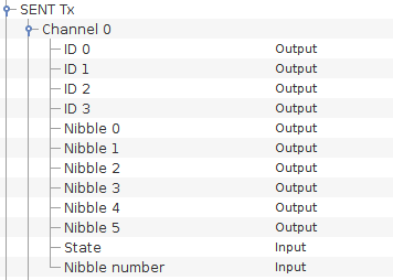
I/O Mapping > SENT Transmitter:
- ID #: Based on the type and num of short/enhanced selection in the IP module configuration panel 1 tp 512 ID # nodes appear here which corresponds to the ID-Data to be transmitted.
Map an Analog IO point which contains the data corresponding to the ID.
- Nibbble #: Based on the num of data nibbles selection in the IP module configuration panel 1 to 6 Nibble # nodes appear here which are the data nibbles to be
transmitted. Map an Analog IO point which contains the data to be transmitted.
- State: The field state indicates the current pulse being sent out and takes values 1-Synchronization pulse, 2-Nibbles,
3-Pause pulse, A-Tick length undefined, B-Low tick undefined, C-Data nibble count undefined or out or range, D-FIFO empty, F-Transmitter disabled.
- Nibbble number: The field nibble number indicates which data nibble is being transmitted and takes values 0-Status and Communication nibble, 1-Data nibble 1,
2-Data nibble 2, 3-Data nibble 3, 4-Data nibble 4, 5-Data nibble 5, 6-Data nibble 6, 7-CRC Checksum nibble.
|
 |
|
|
I/O Mapping > SENT Receiver:
- ID #: Based on the type and num of short/enhanced selection in the IP module configuration panel 1 tp 512 ID # nodes appear here which corresponds to the ID-Data to be received.
Map an Analog IO point to receive to data corresponding to the ID.
- Nibbble #: Based on the num of data nibbles selection in the IP module configuration panel 1 to 6 Nibble # nodes appear here which are the data nibbles received.
Map an Analog IO point to receive the data nibble in.
- Error rate: Error rate indicates the number of packet misses divided by the number of packet hits.
|
 |
|
|
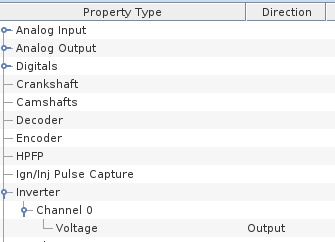
I/O Mapping > Inverter:
- Voltage: Input a value in volts. This value is the input voltage to the Inverter.
|
 |
|
|
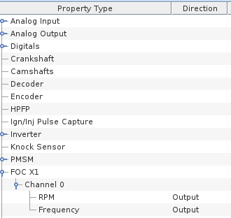
I/O Mapping > Field Oriented Control X1:
- RPM: This is the desired speed for the motor in radians per second. The user input a speed in revolutions per minute which
is converted to a speed in radians per second and programmed.
- Frequency: The Phase Increment is used to generate the triangular wave inside of the 3-phase PWM logic.
|
 |
|
|
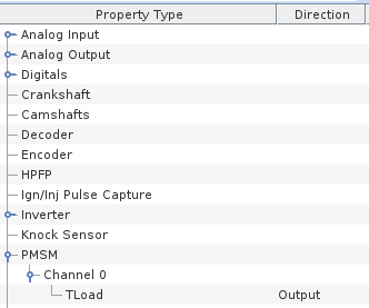
I/O Mapping > PMSM Electric Motor:
- TLoad: Load attached to the PMSM Rotor in Newton Meter.
|
 |
|
|
I/O Mapping > LVDT/RVDT Tx:
- Frequency: Internal excitation frequency for the LVDT/RVDT Tx IP Core in Hertz.
- Data: Data is the information input and takes value -1 to +1 on LVDT mode and data is the theta input in degrees and takes value 0 to 360 on RVDT mode. The data register mode should be set to 1 in the Configuration pane prior.
|
 |
|
|
I/O Mapping > Resolver Tx:
- Frequency: Internal excitation frequency for the Resolver Tx IP Core in Hertz.
- Data: Data is the theta input to be written to the data register and takes value 0 to 360 in degrees. The data register mode should be set to 1 in the Configuration pane prior.
|
 |
|
|
I/O Mapping > Synchro Tx:
- Frequency: Internal excitation frequency for the Synchro Tx IP Core in Hertz.
- Data: Data is the theta input to be written to the data register and takes value 0 to 360 in degrees. The data register mode should be set to 1 in the Configuration pane prior.
|
 |
|
|
I/O Mapping > Multiplexer:
- Control: Each Multiplexer channel has 96 Muxes. Control takes value 0 to 127 because each Mux has maximum of 128 input states.
This value selects which one of input lines is passed on to the output.
|
 |
|
|
I/O Mapping > SIO Tx:
- Count: Cumulative packet count which increments each time data is transmitted. Map an analog output variable of type llong to this field.
- Data: Data contains the data to be transmitted. It is a vector of size 384. Map an analog output vector of type uint and size 384 to this field.
- Ntx_packets: Number of packets transmitted in the data frame. It takes value 1 to 3. Map an analog output variable of type uint to this field.
- Nwords_packet0: Number of words in the first packet transmitted in the data frame. It takes value 1 to 128. Map an analog output variable of type uint to this field.
- Nwords_packet1: Number of words in the second packet transmitted in the data frame. It takes value 1 to 128. Map an analog output variable of type uint to this field.
- Nwords_packet2: Number of words in the third packet transmitted in the data frame. It takes value 1 to 128. Map an analog output variable of type uint to this field.
- Frame Count: Frame count is the number of data frames between SYNCn pulses. If nframes_per_syncn field is set to 2 then this will count from 0 to 1. Map an analog input variable of type uint to this field.
- RCIM edge count: RCIM edge count is the number of rcim pulses between every data frame. If nrcim_pulses is setto 9(which means data gets transmitted every 10 RCIM pulses) then
this will count from 0 to 9. Map an analog input variable of type uint to this field.
|
 |
|
|
I/O Mapping > SIO Rx:
- Count: Cumulative packet count which increments when there is a new data received. Map an analog input variable of type llong to this field.
- Data: Data is a vector of size 1024 which contains the data received. Map an analog input variable of type uint and size 1024 to this field.
- Clear Count: Clear count is a variable that has to changed by the user as an indicator for the IO task to clear the data and the meta data vectors. Toggling this value or incrementing this value will clear the vectors.
Map an analog input variable of type uint to this field.
- Nwords per packet: Meta data vector of size 1024 where each index corresponds to the packet instance received and contains the number of words in that packet. It takes value 1 to 128. Map an analog input
variable of type uint and size 1024 to this field.
|
 |
|
|
I/O Mapping > LVDT/RVDT Rx:
- Distance/Angular Position(deg): In LVDT mode, this contains the vs2-vs1 value and it ranges from -1 to +1. In RVDT mode, this contains the current position of the RVDT as it spins and the value ranges from -90 to +90 degrees.
- Speed(deg/sec): TBD
- RPM: TBD
- Direction: TBD
|
 |
|
|
I/O Mapping > Resolver Rx:
- Angular Position(deg): Angular position is the current position of the Resolver Rx IP Core channel as it spins. The value ranges from 0 to 360 degrees.
- Speed(deg/sec): Angular velocity of the Resolver Rx IP Core channel in degrees per second.
- RPM: Speed in revolutions per minute.
- Direction: Direction represents if its rotation is in clockwise or anti-clockwise. A value of 1 indicates clockwise and a value of 0 indicates anti-clockwise.
|
 |
|
|
I/O Mapping > Synchro Rx:
- Angular Position(deg): Angular position is the current position of the Synchro Rx IP Core channel as it spins. The value ranges from 0 to 360 degrees.
- Speed(deg/sec): Angular velocity of the Synchro Rx IP Core channel in degrees per second.
- RPM: Speed in revolutions per minute.
- Direction: Direction represents if its rotation is in clockwise or anti-clockwise. A value of 1 indicates clockwise and a value of 0 indicates anti-clockwise.
|
 |
|
|
I/O Mapping > Register Write:
- Data: Data to be written to the register after float to fixed-point conversion.
- Data programmed: Actual data written to the register which satisfies the parameters specified in the configuration panel.
For example: If the number of bits is 8, number of intger bits is 3, data type is unisgned and the user is trying to program
a value of 8 then the actual value programmed is 7.96875 because we have only 3 bits to represent the integer part.
|
 |
|
|
I/O Mapping > Register Read:
- Data: Data read from the register.
|
 |
|
|
I/O Mapping > N-Phase Wave Gen:
- Amplitude (0 to N-1): Amplitude of each of the N waveforms to be generated. It takes value -1 to +1.
A value of 1 will result in peak output voltage which is either +5V or +10V depending on the DAC configurations.
- Phase (0 to N-1): Phase of each of the N waveforms to be generated. It takes value -360 to +360 degrees.
- Frequency (Hz): Frequency as an analog output (AO) is the phase increment of the IP Core Channel in Hertz. .
|
 |
|
|
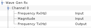
I/O Mapping > Wave Gen Rx:
- Frequency Rx(Hz): Frequency estimate of the input sinusoidal signal in Hertz.
- Magnitude: Amplitude estimate of the input sinusoidal signal. It takes value [-1 to +1].
- Frequency Tx(Hz): Frequency as an analog input (AI) is the phase increment of the carrier input in Hertz.
It takes value 300Hz to 13000Hz.
|
 |
|
|
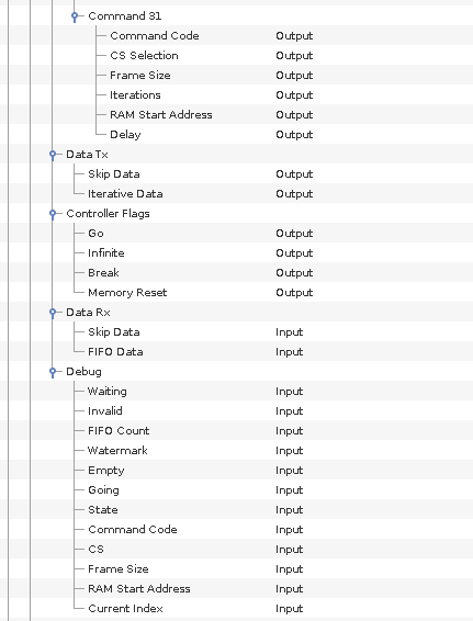
I/O Mapping > SPI Master:
- Command(0 to 31): The SPI Master can execute a maximum of 32 commands in a function call and hence 32 commands in the command list
and each command has the following 6 parameters.
- Command Code: Command Code identifies the operation mode the controller should perform. It takes value 1 for SKIP transmit(Single)
and 3 for Iterative transmit.Map a Unsigned integer variable of size 1 to this node.
- CS Selection: CS Selection identifies the CS DIO line and parameters to use during transmission. It takes value 0 to 5.
Map a Unsigned integer variable of size 1 to this node.
- Frame Size: Frame Size identifies the number of packets in each frame during Iterative mode of transmission. It takes value 1 to 64.
Map a Unsigned integer variable of size 1 to this node.
- Iterations: Iterations identifies the number of times the frame is transmitted during Iterative mode of transmission. It takes a 32
bit integer value.Map a Unsigned integer variable of size 1 to this node.
- RAM Start Address: RAM Start Address indicates the starting offset in RAM to be used for transmission of data using iterative mode.
Each CS can have a maximum of 64 packets and has 64 registers in RAM so this takes value 0 to 63.Map a Unsigned integer variable of size 1 to this node.
- Delay: Delay determines the amount of time between two consecutive commands in the command list and is based on SCK Clk cycles.
Map a Unsigned integer variable of size 1 to this node.
- Data Tx: --
- Skip Data: Skip Data is an integer array of size 6 and indicates the data transmitted on SKIP mode for each of the six CS. Map a Integer vector of size 6 to this node.
- Iterative Data: Iterative Data is a data written to the RAM on Iterative mode. Each CS has maximum of 64 frame size and hence index 0 to 63
corresponds to CS0, index 64 to 127 corresponds to CS1 and so on. Map a Integer vector of size 384 to this node.
- Controller Flags: --
- Go: Go when set to 1 instructs the controller to begin a function if the waiting flag is 1. Map a Unsigned integer variable of size 1 to this node.
- Infinite: Infinite when set to 1 instructs the controller to transmit data continuously based on the controller command list settings. Map a Unsigned integer variable of size 1 to this node.
- Break: Break when set to 1 instructs the controller to complete after the end of a transmission packet, hence interrupting the function.
Map a Unsigned integer variable of size 1 to this node.
- Memory Reset: Memory Reset when set to 1 resets the contents of the FIFO. Map a Unsigned integer variable of size 1 to this node.
- Data Rx: --
- Skip Data: Skip data is as integer array of size 7, index 0 to 5 contains the last data received from each of the six CS on SKIP mode
and index 6 contains the last SKIP data received. Map a Integer vector of size 7 to this node.
- FIFO Data: FIFO data contains the data from FIFO received on Iterative mode of data transfer. Map a Integer vector of size 1504 to this node.
- Debug: --
- Waiting: Waiting when set to 1 indicates that the controller is in idle state waiting for new function and Go flag to be asserted. Map a Unsigned integer variable of size 1 to this node.
- Invalid: Invalid when set to 1 indicates that the total input command count is greater than the total output command count+1 at the beginning of a function.
Map a Unsigned integer variable of size 1 to this node.
- FIFO Count: FIFO Count indicates how many words in the FIFO. Map a Unsigned integer variable of size 1 to this node. Map a Unsigned integer variable of size 1 to this node.
- Watermark: Watermark flag when set to 1 indicates that the FIFO is holding a total number of data greater than the programmed watermark. Map a Unsigned integer variable of size 1 to this node.
- Empty: Empty when set to 1 indicates that the FIFO is empty. Map a Unsigned integer variable of size 1 to this node. Map a Unsigned integer variable of size 1 to this node.
- Going: Going flag indicates if the previous command list is executing or not. A value of 1 indicates that the controller is still executing the previous command list configured
and a value of 0 indicates otherwise. Map a Unsigned integer variable of size 1 to this node.
- Command Code: Command code identifies the operation mode the controller is currently doing. It shows value 1 for SKIP transmit(Single) and 3 for Iterative transmit.
Map a Unsigned integer variable of size 1 to this node.
- CS: CS Selection identifies the CS communicating with the SPI Master. It shows values 0 to 5 indicating CS line 0 to 5. Map a Unsigned integer variable of size 1 to this node.
- Frame Size: Frame Size indicates the number of packets in each frame during Iterative mode of transmission for the command being executed by the controller. It shows value 1 to 64.
Map a Unsigned integer variable of size 1 to this node.
- RAM Start Address: RAM Start Address indicates the ram start address of the current command being executed. It takes value 0 to 63 since each slave can have 64 registers in the controllers RAM.
Map a Unsigned integer variable of size 1 to this node.
- Current Index: Current Index indicates the command number currently being executed. It takes valeue 1 to x where x is the number of commands in the command list.
Map a Unsigned integer variable of size 1 to this node.
|
 |
|
|
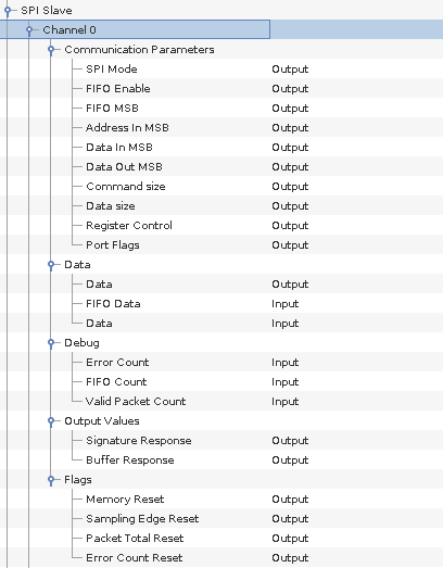
I/O Mapping > SPI Slave:
- Communication Parameters: --
- SPI Mode: SPI Mode identifies the polarity and phase mode the SCK and MISO will be expected. The MSB bit is considered the CPOL bit commonly used in spi mode determination
as the SCK is idle HI when MSB bit is set to 1 and idle LO when MSB bit is set to 0. The LSB bit is considered the CPHA phase bit for SPI SCK control. When LSB bit is set to 1 the
sampling phase is offset to the 2nd edge and when set to 0 the sampling edge is set to the first edge. Map a unsigned integer variable of size 1 to this node.
- FIFO Enable: FIFO Enable dictates whether the FIFO stores or ignores the received SPI data. It takes value 1 for storing data and 0 otherwise. Map a unsigned integer variable of size 1 to this node.
- FIFO MSB: FIFO MSB is the programmable endian of the entire packet data being stored in the FIFO. If takes value 0 or 1 and when set to 1 the first received bit is stored as the MSB and if 0 LSB.
Map a Unsigned integer variable of size 1 to this node.
- Address In MSB: Address In MSB is the programmable endian of write command input address. It takes value 0 or 1 and if set to 1 the MSB is input first. Map a Unsigned integer variable of size 1 to this node.
- Data In MSB: Data In MSB is the programmable endian of write command input data. It takes value 0 or 1 and if set to 1 the MSB is input first. Map a Unsigned integer variable of size 1 to this node.
- Data Out MSB: Data Out MSB is the programmable endian of the read command output data. It takes value 0 or 1 and if set to 1 the MSB is output first. Map a Unsigned integer variable of size 1 to this node.
- Command Size: Command Size is the size of the command portion of the expected packet. It takes value 1 to 16. Map a Unsigned integer variable of size 1 to this node.
- Data Size: Data Size is the size of the data portion of the expected packet. It takes value 1 to 16. Map a Unsigned integer variable of size 1 to this node.
- Register Control: Register Control controls how the data reaches the 128 SPI data registers. When the bit is set to 1, the registers can only be written to through the avalon slave bus, and when set to 0
they can only be written to through SPI commands. This bit is overidden by the individual register port flags if the register is ported out to have a 16-bit input bus externally then this bit is ignored for that particular register.
Map a Unsigned integer variable of size 1 to this node.
- Port Flags: Port Flags is a 128 size array and acts as individual flags that control the input source for each of the 128 16 bit data registers. When set to 1 the data in the respective registers will constantly be
updated to be equal to the value of the unique 16-bit input data bus that is tied to each registers. Map a Unsigned integer vector is size 128 to this node.
- Data: --
- Data: Data is an array of size 128 and contains the 16 bit data written to the SPI data registers using the avalon bus. Map a Unsigned integer vector of size 128 to this node.
- FIFO Data: FIFO Data is an 32 bit integer array of size 1968 and contains the data received from the SPI Master and recorded in the FIFO. Map a Unsigned integer vector of size 1968 to this node.
- Data: Data is an array of size 128 containing the read-back of the 128 16 bit SPI data registers which indicates the data received from avalon bus(register control mode 1) or via ports connected to the respective registers.
Map a Unsigned integer vector of size 128 to this node.
- Debug: --
- Error Count: Error Count indicates the running total of the number of packets detected with an incorrect amount of SCK clock cycles within the bounds of the defined CS.
Map a Unsigned integer variable of size 1 to this node.
- FIFO Count: FIFO Count indicates the running total of the number of packets stored as 32 bit words in the FIFO. Map a Unsigned integer variable of size 1 to this node.
- Valid Packet Count: Valid Packet Count indicates the running total of the number of packets detected with an accurate amount of SCK clock cycles within the bounds of the defined CS.
Map a Unsigned integer variable of size 1 to this node.
- Output Values: --
- Signature Response: Signature Response is the data output through SOMI while the slave is listening for the first command number of bits at the beginning of the packet.
This value being programmed is not necessary to the functionality of the SPI Slave, but functions as an acknowledgement from the slave that the packet has begun. Map a Unsigned integer variable of size 1 to this node.
- Buffer Response: Buffer Response is the data output through SOMI while the slave is listening for the first input data in the second half of a write command packet. This value being
programmed is not necessary to the functionality of the SPI Slave, but functions as an acknowledgement from the slave that the write function is being executed. Map a Unsigned integer variable of size 1 to this node.
- Flags: --
- Memory Reset: Memory Reset takes value 0 or 1 and when set to 1 resets the FIFO. Map a Unsigned integer variable of size 1 to this node.
- Sample Edge Reset: Sample Edge Reset takes value 0 or 1 and when set to 1 resets the sampling edge count register to zero. Map a Unsigned integer variable of size 1 to this node.
- Packet Total Reset: Packet Total Reset takes value 0 or 1 and when set to 1 resets the valid packet count register to zero. Map a Unsigned integer variable of size 1 to this node.
- Error Count Reset: Error Count Reset takes value 0 or 1 and when set to 1 resets the packet error count register to zero. Map a Unsigned integer variable of size 1 to this node.
|
 |
|
|
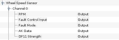
I/O Mapping > Wheel Speed Sensor:
- RPM: RPM is the number of revolutions per minute, positive means forward rotation and negative means reverse rotation.
- DF11 strength: DF11 strength which indicates magnetic field strength that affects the pulses output from the protocol. It takes value 0 to 2, 0 indicates very low magnetic field,
1 indicates normal magnetic field and 2 indicates very high magnetic field.
- AK data: AK data is a 9 bit unsigned integer where each bit can be one of the following software[x], direction, direction valid, hres_index[2], hres_index[1], hres_index[0], standstill, parity.
- Fault control input: Fault control input is the controller of fault and takes values 0 or 1, for all protocols when this bit is set to 1 the wheel and transmitters enact a fault.
- Fault mode: Fault mode decides the way the wheel behaves during a fault of the protocol. It takes value 0 to 3, 0 indicates wheel angle and magnet index go to zero until fault ends, 1 indicates
wheel angle and magnet index return to starting position, 2 indicates wheel angle and magnet index freeze in current position, 3 indicates wheel angle and magnet index continue normal operation.
|
 |
|
|
|